GRIMES COUNTY, TEXAS — The most shocking thing about Elon Musk’s next factory is not that it could cost as much as $119 billion.
It is not that the proposed manufacturing complex could eventually contain more than 100 million square feet of manufacturing space.
It is not even that the facility is being designed to manufacture the silicon brains for Tesla’s autonomous vehicles, Optimus humanoid robots and SpaceX’s planned space-based computing infrastructure.
The most shocking thing appeared almost by accident.
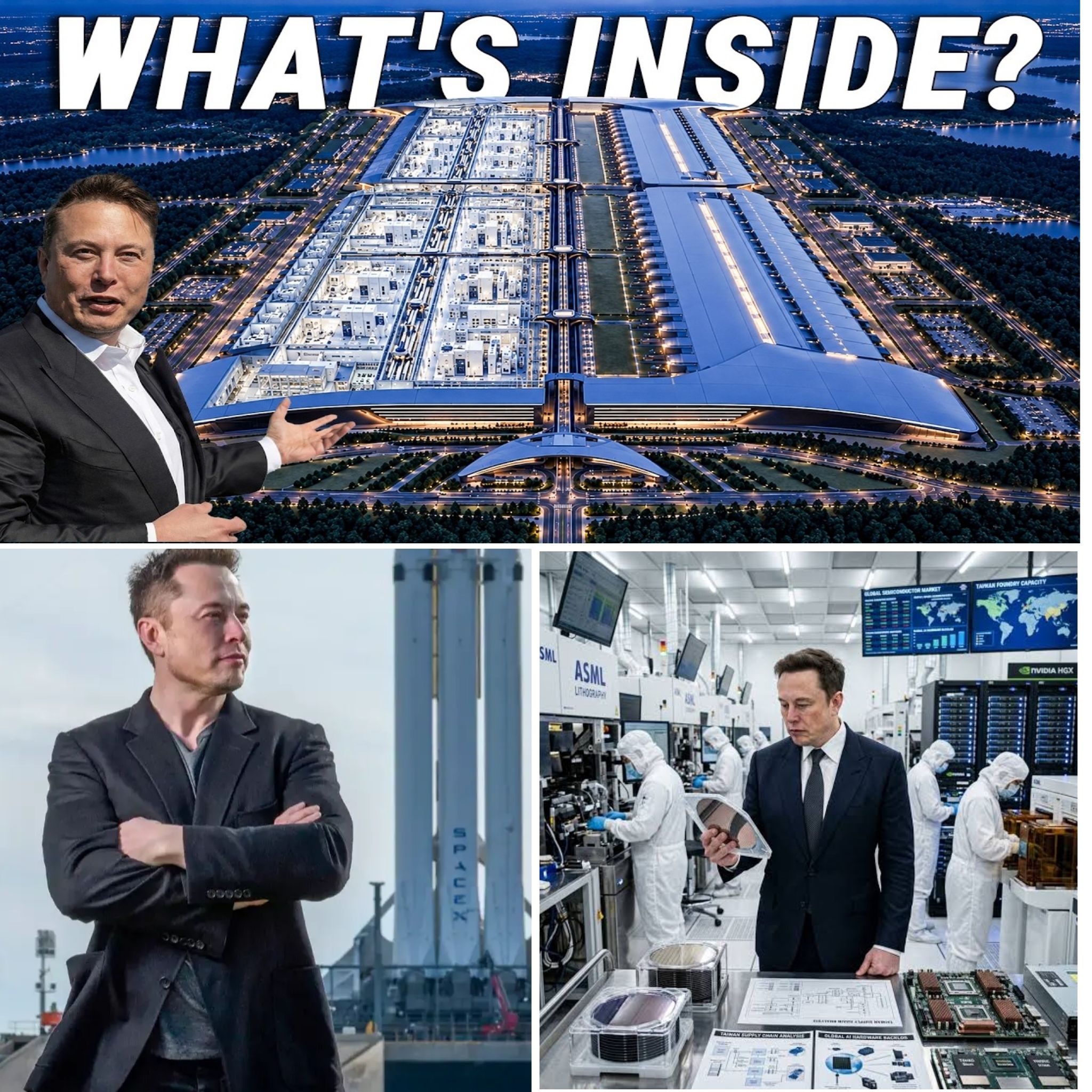
On August 6, a conceptual image of the enormous Texas semiconductor project began circulating online. Engineers and technology watchers immediately noticed something strange near its center: a giant circular structure that did not look like anything normally associated with a conventional chip factory.
One observer asked the obvious question.
Was there a particle accelerator underneath it?

Another went further, wondering whether Musk planned to build a free-electron laser, or FEL, capable of generating extreme-ultraviolet light for semiconductor lithography.
Musk responded with just six characters:
“FEL FTW.”
Free-electron laser. For the win.
Six characters were enough to send a wave through the semiconductor world.
Because if Musk was merely expressing enthusiasm for FEL technology, it was interesting.
If he was hinting that Terafab might eventually experiment with FEL-based EUV lithography, it was extraordinary.
And if the strange circular structure really is connected to such a system—something that has not been confirmed in SpaceX’s filings or technical disclosures—then Musk may not simply be attempting to build one of the largest semiconductor factories ever conceived.
He may be attempting to redesign how a semiconductor factory works.
That distinction changes everything.
And it is where the $119 billion story becomes much stranger.
THE FIRST TWIST: THE $119 BILLION FACTORY IS REAL — BUT THE $119 BILLION ISN’T A CHECK MUSK HAS ALREADY WRITTEN
For months, the number followed Terafab everywhere:
$119 billion.
It sounded almost absurd.
For comparison, that is not the normal price of one semiconductor factory. It is the kind of capital figure normally associated with national industrial strategies, multi-site manufacturing programs or years of investment by the world’s largest chip companies.
Yet the number did not originate from a random social-media account.
A Grimes County public-hearing notice identified SpaceX as the applicant for a proposed “multi-phase, next-generation, vertically integrated semiconductor manufacturing and advanced computing fabrication facility.” It estimated $55 billion for initial phases and $119 billion if additional phases were built.
But here is the first important plot twist.
That does not mean SpaceX has already committed $119 billion.
When Texas Governor Greg Abbott officially announced the Grimes County project on August 6, the first phase was described as an investment of more than $16.8 billion, expected to create approximately 3,000 jobs. SpaceX separately said that future expansion could take investment much higher.
And the legally binding floor is lower again.
According to the agreement reported by local station KBTX, SpaceX committed to invest at least $5 billion by 2030 and create at least 1,800 full-time jobs by 2035. The agreement also contains an exit mechanism allowing SpaceX to terminate under specified conditions.
So the viral headline—“Musk is building a $119 billion factory”—needs one crucial sentence attached to it:
$119 billion is the potential scale of the full multi-phase vision, not money already spent.
That correction makes the story less sensational for about thirty seconds.
Then you look at what they are actually planning.
And it becomes more sensational again.
SpaceX says Terafab is planned as a vertically integrated factory containing more than 100 million square feet of manufacturing space, combining advanced logic, memory, packaging and testing. The company says chips from the complex are intended for hardware including Tesla’s Optimus robots and self-driving Cybercabs, as well as high-power processors for SpaceX’s proposed space-based data centers.
This is not simply “Tesla decides to make its own chips.”
It is an attempt to compress an enormous portion of the semiconductor supply chain into a single industrial ecosystem.
And the reason Musk believes he needs it comes down to a problem money alone cannot fix.
THE CHIP SHORTAGE MUSK SAYS MONEY CAN’T SOLVE
Most companies facing semiconductor shortages do one of four things.
They place larger orders.
They sign longer contracts.
They pay suppliers more.
Or they diversify suppliers.
Musk’s companies are already doing versions of that.
In 2025, Tesla struck a deal valued at roughly $16.5 billion with Samsung for next-generation AI chips. Musk said Samsung’s Texas fab would manufacture Tesla’s AI6 processor, while TSMC was set to manufacture AI5 chips first in Taiwan and later in Arizona.
Ordinarily, that would look like a massive supply agreement.
To Musk, it apparently still did not solve the long-term problem.
During Tesla’s first-quarter 2026 earnings call, Musk explained the reasoning with unusual simplicity: as Tesla and his other companies scale, he said he does not see a path to obtaining enough efficient AI chips from the existing industry.
His phrase was that they would eventually “hit a wall.”
SpaceX has since put an even bigger number on the problem.
The company says combined Tesla and SpaceX requirements could eventually exceed one terawatt of compute, a level it describes as substantially larger than current global supply.
That is the real reason Terafab exists.
Not because Samsung is incompetent.
Not because TSMC is refusing to sell Musk chips.
Not because Tesla suddenly decided semiconductor manufacturing looked fun.
The problem is that Musk’s future-product roadmap, taken literally, implies a demand curve that conventional supplier relationships may struggle to satisfy.
Consider what those products are supposed to do.
A future autonomous Cybercab has to continuously interpret information from cameras and other systems while making decisions in real time. It cannot tell a passenger, “Please wait four seconds while the cloud finishes processing this intersection.”
An Optimus humanoid robot has an even stranger workload.
Driving occurs in an environment built for vehicles: roads, lanes, signs, traffic rules.
A humanoid robot is expected to enter an environment built for humans.
Chairs move.
Objects fall.
Children walk unexpectedly through rooms.
Someone leaves a bag on the floor.
A cup is placed five centimeters away from where it was yesterday.
The robot has to perceive, infer, balance, plan and react continuously.
Then there is SpaceX.
Its ambitions increasingly extend beyond using satellites as communications relays. SpaceX has publicly discussed AI compute satellites and says its future architecture could place substantial computing capability in orbit, connected by laser links and supported by Starlink infrastructure.
Now combine those three worlds:
Autonomous transportation.
Humanoid robotics.
Orbital AI.
Suddenly, semiconductor supply is not simply another line on a procurement spreadsheet.
It becomes the ceiling on the entire Musk industrial ecosystem.
If that interpretation is correct, whoever controls the chips controls the speed at which everything else can scale.
So Musk’s answer is classic vertical integration taken to an almost uncomfortable extreme:
If the supply chain becomes the bottleneck, absorb the supply chain.
But semiconductor manufacturing has a brutal history of punishing companies that believe money and ambition are sufficient.
That is why some experts see Terafab and do not see a revolution.
They see a trap.
THE FACTORY THAT CHIP ENGINEERS SAY SHOULD TERRIFY ITS OWN BUILDERS
There is something deceptive about semiconductor manufacturing from the outside.
A photograph of a fab looks calm.
White floors.
White walls.
Workers in cleanroom suits.
Robotic wafer carriers moving almost silently above expensive equipment.
Nothing resembles a steel mill or an automobile stamping line.
But that cleanliness hides violence at the atomic scale.
To make an advanced processor, manufacturers repeatedly deposit material, remove material, pattern material, measure it, polish it and repeat the process across hundreds or even thousands of highly controlled operations.
Tiny variations compound.
A contamination problem too small for a human eye to perceive can destroy yield.
Temperature moves dimensions.
Vibration matters.
Chemical purity matters.
Alignment errors measured at nearly unimaginable scales matter.
And then comes the most dangerous word in chip manufacturing:
yield.
You can make a technically functioning processor and still lose billions.
The question is not simply whether one chip works.
The question is whether enough chips on enough wafers work, repeatedly, across enormous production volumes, at a cost low enough to justify the factory that produced them.
That knowledge is not contained in a blueprint.
Much of it exists in the accumulated experience of engineers who have watched thousands of process failures, learned which machine readings matter, discovered which variables interact and gradually pushed a manufacturing line from “technically possible” to “commercially reliable.”
That expertise takes decades to build.
It is one reason a detailed Tom’s Hardware analysis of Musk’s original Terafab vision concluded that the full ambition looked extraordinarily difficult, describing barriers involving capital, equipment, workforce and semiconductor-manufacturing expertise that make the largest versions of the plan unrealistic on normal industry timelines.
This is where Musk’s normal industrial playbook encounters something different.
Tesla could redesign cars around manufacturing.
SpaceX could rethink rockets around reusability.
But advanced semiconductor production contains an ecosystem of dependencies that no single factory automatically controls.
Lithography.
Photoresists.
Masks.
Etch tools.
Deposition systems.
Metrology.
Inspection.
Ultra-pure chemicals.
Vacuum systems.
Packaging.
Memory.
Specialty gases.
Precision optics.
And armies of engineers who understand how all those systems misbehave together.
You can buy the machines.
You cannot place an order for “30 years of institutional memory, delivered Thursday.”
And then Musk posted those six characters.
FEL FTW.
That is when Terafab stopped looking merely enormous.
It started looking experimental.
THE CIRCLE IN THE MIDDLE OF TERAFAB
To understand why Musk’s FEL response created such excitement, you have to understand the strangest machine at the heart of modern advanced chip manufacturing.
The world’s leading-edge chipmakers depend heavily on extreme-ultraviolet lithography, or EUV.
EUV lithography uses light with a wavelength of about 13.5 nanometers to help pattern extraordinarily tiny features onto wafers.
Producing that light reliably is almost ridiculous.
Inside current ASML EUV systems, microscopic droplets of tin travel through a vacuum chamber.
A powerful laser targets them.
Not occasionally.
ASML says its system can fire at droplets 50,000 times every second, generating a plasma that emits EUV radiation. Mirrors then collect and guide that light toward the wafer.
Pause on what that means.
Someone had to build a machine capable of identifying microscopic tin droplets traveling through a vacuum and hitting each one with precisely timed laser pulses tens of thousands of times per second.
And that is just the light source.
The rest of the lithography system must manipulate wafers and masks with precision measured in fractions of a nanometer while managing heat, vibration, vacuum conditions and optical distortion.
This is why ASML occupies one of the strangest strategic positions in the modern technology economy.
Its EUV machines are not simply “better printers.”
They are among the most complicated pieces of industrial equipment humans have ever manufactured.
Which raises the question:
Why would anyone try something different?
Because the current system is brilliant—but it is also brutally complicated.
Tin is necessary for generating the light, yet it also creates contamination-management challenges. ASML itself describes tin management as a unique engineering problem because the material is simultaneously essential and potentially harmful to optics.
A free-electron laser offers a completely different conceptual route.
Instead of generating EUV by blasting tin droplets into plasma, an FEL accelerates electrons to extremely high energies and passes them through alternating magnetic structures called undulators.
The interaction can produce highly intense, tunable electromagnetic radiation.
FELs already exist.
Particle accelerators already exist.
The physics is not science fiction.
The question is whether an FEL can become a reliable, economically sensible industrial EUV source operating around the clock inside a high-volume semiconductor environment.
Those are profoundly different standards.
A physics laboratory can tolerate experiments.
A factory cannot tolerate surprises.
THEN CAME THE SECOND TWIST: MUSK ISN’T THE ONLY ONE TAKING FEL SERIOUSLY
For several days, the obvious response to the FEL speculation was:
Interesting idea.
Probably internet overinterpretation.
Then another fact made the whole story harder to dismiss.
A U.S. startup called xLight is already developing a free-electron-laser-based alternative source for EUV semiconductor lithography.
And this is not a garage experiment funded by an anonymous crypto millionaire.
Former Intel CEO Pat Gelsinger serves as executive chairman of xLight.
More importantly, in June 2026, the U.S. Department of Commerce and the National Institute of Standards and Technology finalized $150 million in CHIPS Act incentives to support construction and demonstration of xLight’s FEL prototype at the Albany Nanotech Complex in New York.
Suddenly Musk’s cryptic reply looked different.
It still did not confirm Terafab would use an FEL.
That distinction matters.
No detailed public Terafab filing identified a working FEL lithography architecture, beam specification, industrial deployment schedule or production-ready accelerator system.
“FEL FTW” is evidence that Musk is interested in the technology.
It is not evidence that the mystery circle in the rendering is a finalized particle accelerator.
But it means the underlying idea is not fantasy.
There is a genuine technological race here.
And that opens an extraordinary possibility.
Imagine one giant centralized EUV source supplying light to multiple lithography stations.
In a normal mental model, every advanced lithography machine is largely its own self-contained universe.
But what if light generation became shared infrastructure?
Electricity is generated centrally and distributed.
Water is processed centrally and distributed.
Industrial gases are generated or stored and distributed.
So what if extreme-ultraviolet light itself could someday be treated as a factory utility?
One massive source.
Multiple endpoints.
That is the theory behind some of the excitement surrounding FEL and the unusual Terafab rendering.
If it worked, the architecture could alter the economics of extreme-scale chip manufacturing.
But there is a brutal downside.
A centralized system also creates a centralized failure mode.
When one scanner’s source has a problem, you lose one scanner.
If one experimental central source feeds many scanners and that source fails, you could potentially disrupt a much larger percentage of production.
The technology that promises to remove a bottleneck could become the biggest bottleneck in the building.
That is why semiconductor veterans remain cautious.
The demonstration is not the product.
The prototype is not the fab.
And the fab is not the yield curve.
THE THIRD TWIST: MUSK APPEARS TO KNOW THAT
The easiest version of this story would portray Musk as recklessly placing $119 billion on an untested semiconductor experiment.
The public evidence points to something more calculated.
Tesla did not immediately leap from zero semiconductor-fab experience to a 100-million-square-foot production monster.
SpaceX said in August that Tesla had already broken ground in April on a research fab at Giga Texas, describing it as a precursor to Terafab.
That matters enormously.
A research fab gives engineers somewhere to fail cheaply—or at least more cheaply than inside a mega-campus.
They can learn equipment behavior.
Develop process recipes.
Recruit manufacturing talent.
Test integration.
Discover what works.
Discover what absolutely does not work.
Then scale what survives.
Tesla has also started hiring people whose résumés suggest the company understands the difference between designing chips and actually producing them.
One of the most notable recruits is Gary Jiang, who spent nearly 18 years at Intel before becoming Tesla’s Director of Tera Fab in 2026. His Intel work included manufacturing preparation and technology transfer associated with the company’s 18A process.
That hire may sound like a small detail beside a $119 billion headline.
It may be one of the most important details in the entire story.
Because the missing ingredient inside Musk’s companies was never ambition.
It was fab experience.
Intel provides another layer of insurance.
In its first-quarter 2026 earnings materials, Intel confirmed its partnership with SpaceX, xAI and Tesla around Terafab and said the companies were exploring ways to rethink silicon process technology and manufacturing economics.
This is not Musk replacing the semiconductor industry overnight.
At least initially, it looks much more like Musk trying to import the semiconductor industry’s knowledge into his vertically integrated structure.
That difference may determine whether Terafab becomes historic—or merely expensive.
And then comes the part almost nobody talks about.
The factory may not actually be a chip project first.
It may be an energy project.
TERAFAB’S REAL PRODUCT MAY BE ELECTRICITY
A semiconductor fab cannot treat electricity the way a normal office building does.
If power flickers in an office, screens go dark.
People complain.
Systems reboot.
In semiconductor manufacturing, unstable power can interrupt tightly controlled process steps and damage work that has already spent days or weeks moving through production.
For a facility on the scale proposed in Grimes County, power quality therefore becomes existential.
Texas also faces rapidly rising electricity demand from AI data centers and industrial development.
SpaceX’s answer is extraordinary in its simplicity:
Bring its own power.
Company representatives said Terafab is expected to rely on on-site natural-gas generation combined with very large battery arrays, rather than depending primarily on the Texas grid. The project’s agreements similarly contemplate natural-gas-fired power plants and battery storage.
That decision produces another reversal in the story.
Musk is famous for Tesla batteries and solar energy.
Yet one of his most ambitious new industrial projects is currently being designed around large-scale natural-gas generation backed by batteries.
Why?
Reliability.
A giant semiconductor factory does not merely need enormous amounts of energy.
It needs extraordinarily predictable energy.
Voltage quality matters.
Interruptions matter.
Restart procedures matter.
Power architecture becomes part of semiconductor yield.
The deeper you examine Terafab, the clearer the pattern becomes.
Musk does not just want control of chip design.
He wants control of chip manufacturing.
But controlling manufacturing is meaningless without controlling power.
And controlling power is meaningless without controlling cooling and water.
Which leads to the next battlefield.
THE FACTORY IS BEING BUILT WHERE A COAL PLANT DIED
The Grimes County site carries an almost cinematic symbolism.
Terafab is tied to the area around Gibbons Creek, the site of a former coal-fired power plant. Public records and local project material describe a vast industrial zone around the former power facility and reservoir.
Old energy infrastructure is being transformed into infrastructure for the AI age.
Coal once moved electrons through transmission lines.
Now the same landscape could manufacture devices that move trillions of calculations through silicon.
The reservoir is important too.
SpaceX says it plans to use Gibbons Creek Reservoir water for industrial operations rather than local groundwater, along with on-site wastewater treatment, reuse and conservation systems.
That promise exists for a reason.
Across the United States, communities hosting AI data centers and semiconductor projects are increasingly asking two uncomfortable questions:
How much electricity will you consume?
And how much water will you take?
Those questions become especially sensitive when the industrial project is larger than anything local infrastructure was originally designed to support.
And Terafab is not arriving quietly.
Local residents have raised concerns about transparency, infrastructure, environmental impacts, farmland and the enormous public incentive packages attached to the project. Local reporting has also documented questions surrounding water rights and records connected with the site.
Supporters see thousands of jobs, a massive tax base and the chance to turn rural Texas into one of the most strategically important semiconductor regions in the world.
Critics see a corporate project so large that local government may struggle to negotiate with it on equal footing.
Both reactions are understandable.
Because Terafab is not merely moving into a community.
At full scale, it could reshape the community around itself.
AND THEN THE STORY LEAVES EARTH
At this point, most people assume they understand the project.
Tesla needs chips.
Cybercab needs chips.
Optimus needs chips.
Build factory.
Problem solved.
Except SpaceX’s own description reveals a different endgame.
Terafab chips are also intended for space-based data centers.
That may turn out to be the biggest twist of all.
Cybercab and Optimus are the visible products.
People can imagine them.
A taxi drives down the street.
A robot folds laundry.
But orbital computing changes the scale of the equation.
SpaceX already operates thousands of Starlink satellites.
Its longer-term AI concept imagines satellites carrying substantial computing hardware, interconnected by optical links, potentially powered in orbit and upgraded in rapid generations.
If SpaceX genuinely attempts to manufacture AI satellites at anything approaching automotive volumes, semiconductor consumption could become enormous.
Now reconsider Musk’s claim that existing chip capacity eventually becomes inadequate.
He is not planning around the number of Teslas sold today.
He is planning around a world in which Tesla manufactures fleets of autonomous machines while SpaceX manufactures fleets of computing spacecraft.
That is a very different demand forecast.
And it explains why normal supply contracts may look insufficient from inside Musk’s planning rooms even when they look gigantic to everyone else.
Terafab, viewed through that lens, is not simply a semiconductor factory.
It is the industrial bridge connecting Earth-based robotics to orbital AI.
That is either breathtakingly visionary or breathtakingly premature.
Possibly both.
THE CHIP IS NOT THE FINAL PRODUCT
There is another reason vertical integration matters.
Price.
Buying advanced processors from outside suppliers means paying for more than silicon.
The supplier must recover research spending, factory investment, equipment depreciation, labor, yield losses and profit.
For most companies, that is perfectly rational.
Building your own advanced fab would be insane.
But vertical integration becomes more attractive when three conditions occur simultaneously:
You consume extraordinary volumes.
You can keep the factory heavily utilized.
And lower semiconductor costs unlock much larger downstream markets.
That is where Cybercab and Optimus become important.
A robotaxi only becomes transformational if the economics beat traditional transportation.
A humanoid robot only becomes a mass-market machine if its computing hardware, actuators, batteries and manufacturing costs fall far below the price of exotic industrial robotics.
If Tesla can reduce the cost of the intelligence inside those machines while simultaneously securing supply, Terafab could influence the entire cost curve.
Not because semiconductor margins disappear.
Owning a fab does not make manufacturing free.
But because Tesla could optimize hardware, software, packaging and production around exactly one family of workloads.
A traditional chip supplier wants a large customer base.
Terafab can theoretically ask a narrower question:
What is the cheapest possible silicon architecture for the machines Musk wants to deploy by the billions?
That is a radically different optimization problem.
And if the answer works, the factory becomes less about selling processors and more about making robots affordable.
But this is also where the story becomes politically uncomfortable.
WHAT HAPPENS IF ONE ECOSYSTEM CONTROLS EVERYTHING?
Imagine the complete stack.
One organization designs the AI workload.
Its partners design the chips.
They manufacture the chips.
They package them.
They install them in autonomous vehicles.
They install them in humanoid robots.
Another Musk-controlled company launches satellite infrastructure connecting those machines.
Space-based computing could process additional workloads.
Software updates move through the ecosystem.
Data from deployed machines helps improve future systems.
Then those improved systems drive the next generation of chips.
That is vertical integration approaching a scale technology companies have rarely possessed.
Supporters will say this is exactly what American industry needs.
They will point to the great vertically integrated industrial companies of history.
Oil companies controlled extraction, refining and distribution.
Steel companies controlled mines, furnaces and transportation.
Telecommunications companies built networks end to end.
Vertical integration can reduce transaction costs, shorten development cycles and remove fragile dependencies.
And there is a national-security argument.
Advanced chips are strategic infrastructure.
A larger domestic manufacturing base reduces dependence on geographically concentrated overseas production.
But critics see the same architecture and reach a very different conclusion.
The concern is not the existence of a robot.
It is concentration of control.
If the same economic ecosystem controls compute, connectivity, autonomous machines and the infrastructure required to manufacture each generation, then decisions once distributed across multiple independent suppliers become centralized.
That raises questions about interoperability.
Competition.
Privacy.
Access.
Data ownership.
Regulatory oversight.
And the ability of users to leave one ecosystem for another.
Those questions do not prove Terafab is dangerous.
But refusing to ask them would be irresponsible.
Industrial history repeatedly shows that infrastructure creates power long after the excitement surrounding its construction disappears.
WHAT ABOUT THE “TESLA PHONE”?
This is where internet speculation goes too far.
The supplied Terafab theory points toward an interesting gap.
Cybercabs could connect through increasingly sophisticated networks.
Optimus is intended to respond naturally to human instructions.
Starlink can provide connectivity in places conventional terrestrial networks cannot easily reach.
One could therefore imagine a simple consumer device serving as a control interface across that ecosystem.
And that possibility has revived the eternal rumor:
Tesla phone.
But there is an important fact that viral posts routinely skip.
There is still no publicly confirmed Tesla smartphone program equivalent to the publicly announced Cybercab, Optimus or Terafab initiatives.
A logical opening in an ecosystem is not evidence that a specific secret product exists.
It is possible Musk’s companies eventually introduce a specialized interface.
It is possible they rely entirely on existing smartphones.
It is possible voice interaction makes another dedicated device unnecessary.
Until Tesla announces something concrete, the “Tesla phone” belongs in the speculation column.
That distinction matters because Terafab is already extraordinary enough without inventing products to make it more dramatic.
THE TWO FUTURES HIDING INSIDE THE SAME TEXAS FIELD
Terafab now appears to contain two completely different futures.
In the first, the skeptics are right.
Construction costs rise.
Advanced equipment arrives more slowly than expected.
Process development slips.
Yields disappoint.
Experienced semiconductor workers prove difficult to recruit in sufficient numbers.
The FEL experiment—if one is actually attempted—remains a laboratory technology instead of becoming a production technology.
One million wafer starts per month remains a presentation target rather than an industrial reality.
The $119 billion maximum buildout is never reached.
Terafab becomes an expensive reminder that semiconductor manufacturing is one of the few industries where even the richest companies cannot simply purchase their way through the learning curve.
Business schools teach the case for decades:
A charismatic industrial empire that believed vertical integration could compress forty years of semiconductor experience into several years—and discovered that physics does not respond to deadlines.
That future is entirely plausible.
But there is another one.
The Austin research fab works.
Intel knowledge transfers successfully.
Veteran engineers build a manufacturing culture.
Early Terafab phases achieve acceptable yields.
Packaging, memory and logic integration shorten design cycles.
Tesla’s processors become cheaper.
Optimus production expands.
Cybercab economics improve.
SpaceX deploys increasingly powerful computing satellites.
The Grimes County campus expands phase after phase.
And perhaps, somewhere along that timeline, an FEL-derived EUV source actually becomes reliable enough for industrial production.
If that happens, then the strange circle that triggered an internet argument in August 2026 will look completely different in retrospect.
It will look like a warning.
Not that ASML suddenly disappears—advanced lithography involves far more than swapping one light source for another, and ASML’s decades of expertise cannot simply be erased by a particle accelerator.
But a successful alternative EUV source could attack one of the most difficult bottlenecks in semiconductor scaling.
More light.
Potentially different economics.
Potentially new factory architectures.
Potentially enormous throughput.
That possibility is exactly why xLight is receiving serious government support.
It is why semiconductor engineers are discussing FEL again.
And it is why Musk’s two-word response mattered.
THE MOST IMPORTANT NUMBER ISN’T $119 BILLION
People will continue arguing about the headline number.
$16.8 billion.
$55 billion.
$119 billion.
One terawatt.
One hundred million square feet.
Thousands of workers.
Eventually, perhaps, up to one million wafer starts per month.
But money may not decide whether Terafab succeeds.
Yield will.
Talent will.
Energy reliability will.
Equipment availability will.
Process discipline will.
And time will.
Those are harder problems because none can be solved by writing one enormous check.
That is also why dismissing Terafab as another Musk publicity stunt may be premature.
The Grimes County project is real.
The incentives are real.
The first-phase announcement is real.
The Austin research fab is real.
The Intel partnership is real.
The semiconductor hiring is real.
The independent FEL race is real.
And Musk really did respond to FEL speculation with:
“FEL FTW.”
What remains unknown is whether all those pieces converge into the machine people think they see.
A factory unlike any fab operating today.
A semiconductor city with its own power infrastructure.
Logic, memory, packaging and testing under one roof.
Processors flowing into cars, robots and satellites.
Perhaps, eventually, an accelerator generating the light used to print parts of the next generation.
That is the part nobody outside the project can responsibly claim to know yet.
And perhaps that uncertainty is what makes Terafab more fascinating than the usual Musk headline.
Because either outcome would be historic.
If it fails at full scale, Terafab could become one of the most expensive lessons ever delivered by the semiconductor industry: proof that accumulated manufacturing knowledge remains more powerful than capital.
If it succeeds, it could demonstrate that the architecture of advanced semiconductor production is not as fixed as the industry assumed—and give Musk’s companies something much more valuable than another factory.
Compute sovereignty.
The ability to design the intelligence.
Manufacture the intelligence.
Power the factory that creates the intelligence.
Connect the machines carrying the intelligence.
And launch some of that intelligence beyond Earth.
That is why calling Terafab merely a “chip factory” may eventually sound as incomplete as calling Starlink a collection of antennas.
The building is not the story.
The system is.
And somewhere inside that proposed system sits a giant unanswered question shaped like a circle.
Was “FEL FTW” simply Elon Musk cheering for an interesting technology?
Or was it the smallest public clue yet to the most radical part of Terafab?
For now, nobody outside the project can prove the answer.
But the concrete is coming.
The engineers are being hired.
The power plans are taking shape.
And the semiconductor industry has started watching.